
![]()
![]()
![]()
![]()
![]()
![]()
Engineering
![]() This page has been provided for design
engineers who wish to send PCB data to us for build. We have
included many helpful tips on how to streamline the process and keep tooling
and manufacturing costs to a minimum. Also, we have included a
comprehensive summary of the engineering process. If you have any
questions, please feel free to contact our Engineering Manager at:
eng@standardpc.com
This page has been provided for design
engineers who wish to send PCB data to us for build. We have
included many helpful tips on how to streamline the process and keep tooling
and manufacturing costs to a minimum. Also, we have included a
comprehensive summary of the engineering process. If you have any
questions, please feel free to contact our Engineering Manager at:
eng@standardpc.com
Incoming Files
When sending files to our engineering
department please email to
eng@standardpc.com in a zipped file to
reduce transmission time. We prefer that files be in a Gerber 274X
format. The 274X format utilizes embedded apertures and saves a great
deal of time over manually entering them off an aperture list. If you
would like to include a blueprint as an AutoCad *.dxf file, this is fine.
Be sure to reference your files with the part number which will be on the PO so we can identify them
easily. We prefer that you use filenames of no greater than 8
characters. We also prefer that at least one layer has the board
boundaries for outside edges and any internal routed features. Be sure
to include contact information in case we need to get a hold of you.
Design Rule Check
After the files have been received, the
next step is to perform a thorough DRC. Design Rule Check allows us to
evaluate the design and its manufacturability through our processes.
Our CAM program has pre-entered min/max values for a host of design
criteria. Although under certain circumstances we can 'stretch' these
rules, we must be able to evaluate each DRC violation to ensure
manufacturability is maintained. If DRC violations exist, we will then
try to resolve these through your engineering department. We have
included below the min/max values that exist in our DRC algorithm so that
you can proactively address these before sending the files. Little or
no DRC violations will help keep the NRE and board manufacturing costs
lower.
SPECIAL NOTE: Please use flashed pads instead of draws whenever possible. It requires additional time for our engineer to convert draws to flash. DRC checks and electrical test generation utilities require that the pads be flashed. Also, when using a polypour or fill routine to create planes, be sure that the borders are completely closed. If not, the fill routine will not work properly. Be sure that all traces terminate at the middle of the pad.
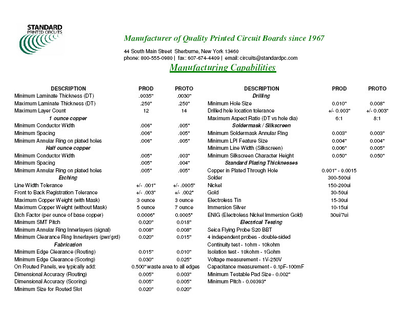
Design Rules for Manufacturabilty (Click here to download a PDF version of this chart)
 |
*Please keep in mind that we clear silkscreen away from all solderable surfaces (PTH and SMT pads) by 3-5 mils. If the designer has placed the silkscreen pattern over solderable surfaces, the clearing routine may affect legibility.
**Etch factor is a reduction of line width due to the etching process. The sides of the copper trace are exposed to the etching solution as the unwanted copper is removed from the surface. The amount of reduction is dependant on the thickness of the base copper cladding. For example: A 10 mil trace may be reduced 0.5 mils when etching 1oz copper clad or 1.0 mil when etching 2oz base copper. Staying within 20% of nominal trace width as specified by IPC is not a problem with standard copper weights. If heavier copper weights are used then compensating the line width may be required to maintain the 20% tolerance. For a 12 mil line utilizing a 4oz copper base, it would be advisable to compensate the designed line width by 2 mils to allow for etch factor.
A similar situation exists with RF designs where line width tolerances are critical to the function of the board. Typically we will compensate line widths as necessary to achieve the designed line width (as taken from the gerber files) after etching. If you would prefer to compensate the line widths yourself, please notify us so we do not over compensate.
***These standard plating thicknesses are what we consider default values if not specified by your documentation. Thinner or thicker coatings are available on all electrolytic processes.
Panelization
Panelization is the layout
of the boards into a scored or routed matrix or array. This is done to
optimize the efficiency of the assembly operation. If you have a
specific panelization requirement, please send a drawing that clearly
illustrates what the panel should look like. We would very much prefer
that you did not provide Gerbers in a panelized format. Generally we
like to produce a finished panel that is approximately 8.0" x 10.5".
This is the most efficient yield from our standard panel size. Below
is a description of the most common panelization methods.
Scored Panel - is an array of boards, zero spaced, held together by a very narrow score cut. The web is approximately 25% of the laminate thickness and snaps apart fairly easily. Scored panels are generally limited to rectangular parts. Circuit features must be a minimum of 0.030" from the board edge.
Routed Panel - is an array of boards, 0.125-0.300" spaced, held together by tabs. The tabs are usually 0.040" wide and there are as many as needed to maintain stiffness and support across the panel. They break apart fairly easily, however, a subsequent grinding operation may be necessary to remove the residual tab material.
Photoplots
After panelization, the
next step is to prepare to send the files for photoplotting.
Photoplots are the tools used to create the images that will be applied to
the boards. The plots consist of silver halide films and are used to
create the diazo film copies that ultimately used for imaging. After
we generate the diazo copies, we ship the silver originals to you.
Net List Test Generation
If the customer requires
electrical testing, the CAM program will be used to extract a net list from
the gerber files. A net is a connection of continuous points and
traces. Each net will be tested to ensure that there is no break in
continuity (resistance) and that it is not shorted to another net (leakage).
The net list will create a drill file from which the test fixture will be
manufactured. Then the net list program is downloaded into the
electrical test equipment in order to create the actual test program.
Drill - Rout - Score Files
Drill programs are
normally extracted from the customer's CAD system and are included with the
's gerber file package. These files must be in ASCII format and
preferably as Excellon compatible. Only minor changes are required to
these in order for us to use. Rout programs are created from the
gerber layer which has the edge borders included. The program
recognizes these borders and creates a rout program from them. Scoring
programs are generated at the CNC controller of the scoring equipment.
Methodologies
The last step taken by
engineering is to create the floor traveler and include all the processes
and methods required by the job. Utilizing our shop floor control,
each job is assigned a 'recipe' of methods which is printed out on the job
traveler. Any required notes or comments are included at each method.
Operators will review these notes before commencing with the job.
Material type, thickness and copper weight is also assigned at this phase.
| home | profile | products | services | laminates | processes | engineering | rfq | contacts |
© 2002, 2007 by Standard Printed
Circuits Inc.
All Rights Reserved