![]()
![]()
![]()
![]()
![]()
Download our FREE Microwave Laminates Comparison Chart. Makes a great reference tool for engineers.
|
|
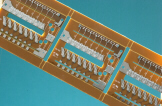
Single-sided PCB |
|
|
Double-sided PCB |
|
|
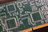
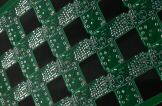
Multilayer PCB |
|
|
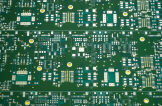
RF/ Microwave |
|
|
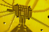
SMOBC-HAL (surface
mount technology SMT) Soldermask Over Bare Copper usually provided with a Hot Air Level (HAL) solder finish which selectively places solder onto pads and holes only. This provides an excellent base for attaching SMD components. |
|
|
Alternative Finishes (Including RoHS Compliant Finishes) We offer a variety of different surface finishes including: Gold, nickel, tin, solder reflow, bare copper with anti-oxidant, silver, and rhodium. Thicknesses can vary according to your specification (see Engineering for default thicknesses). |
|
|
Panelization Options We can provide accurate scored and/or routed arrays to optimize your assembly process. Typically, an 8" x 10" panel is the most cost effective size due to 'best yield' from our standard panel size. |
|
|
High Performance
Laminates From multifunctional epoxy resin systems to high performance polyimide, we offer a wide selection of laminates (see Laminates). Some of the multifunctional epoxies are approaching polyimide in high temperature performance. |
Manufacturing Capabilities:
| Layers: | 1-12 FR4, polyimide, multifunctional, and multilayer RF |
| Lines/Spacings (mils): | 6/6 production, 4/4 prototype |
| SMT minimum pitch (mils): | 18 |
| Minimum finished hole size (mils): | 10 |
| Aspect ratio (max.): | 6:1 |
| Blind / Buried vias | yes, with some restrictions |
| Available finishes: | SMOBC-HAL, solder reflow, electroless tin (20-30 µi), immersion tin (10-15 µi) , nickel, gold, bare copper (with CU-56 antioxidant), immersion silver. |
| Soldermasks: | Liquid Photoimageable (LPI). |
| Soldermask Colors: | green, blue, red, black, clear |
| Silkscreen | Liquid Photoimageable, epoxy based thermal cure. |
| Silkscreen Colors: | white, yellow, black |
| Minimum LPI Mask Resolution (mils): | 4 |
| Copper Foil: | minimum 1/2 oz., maximum 3oz with mask or silk - 5oz without mask or silk |
| Electrical Test: | grid test or flying probe netlist testing |
| Laminate Thicknesses: | 0.005" - 0.250" |
| Lead Times: | single-sided protos - 24-48 hrs. double-sided protos - 48-72 hrs. (includes RF boards) quickturn single and double-sided - 5 days multilayer protos - 5-10 days normal lead times - 2-3 wks note: lead times are calculated from the time the PO is received to the time the product is shipped. If the PO (and gerber files) are received by Noon we will count that as day one. |
| Line width etching tolerances | 1/2 oz. foil - +/- .001", 1 oz foil - +/- .002" |
| Special Processes: | peelable soldermask |
| Panel sizes: | min - 6" x 9", max - 18" x 24" |
| QA / Testing: | Quality system compliant with ISO 9000, inspection to IPC-A-600 (current rev.) Class 2, solderability testing to IPC-TM-XXX, electrical test, cross-sectioning lab, coating thickness testing, PTH thickness testing, calibration system to MIL-STD-45662, UL-94V0 (94V1 for polyimide). |
| home | profile | products | services | laminates | processes | engineering | rfq | contacts |
© 2002, 2007 by Standard Printed
Circuits Inc.
All Rights Reserved